MV6
Jump to navigation
Jump to search
The printable version is no longer supported and may have rendering errors. Please update your browser bookmarks and please use the default browser print function instead.
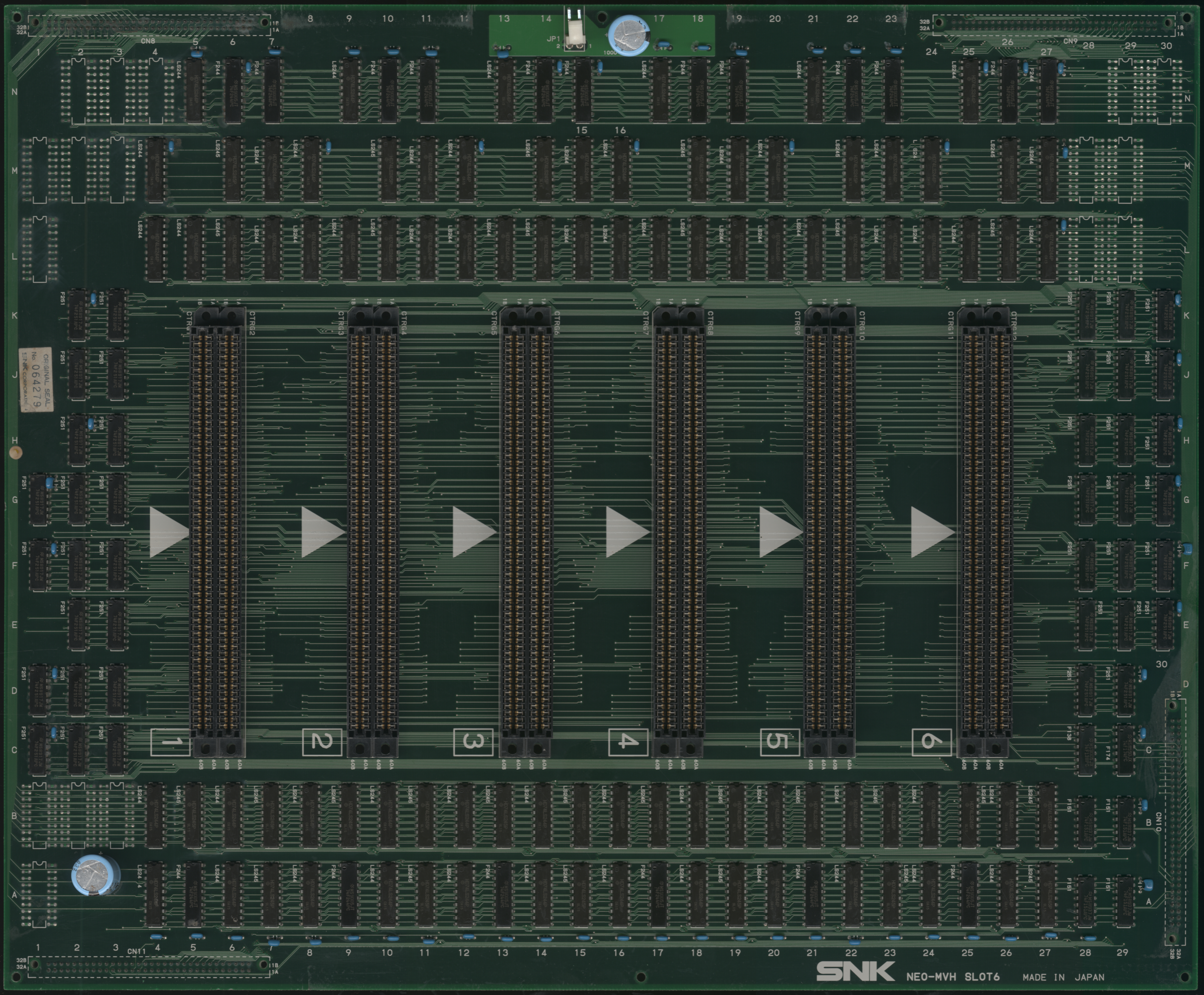
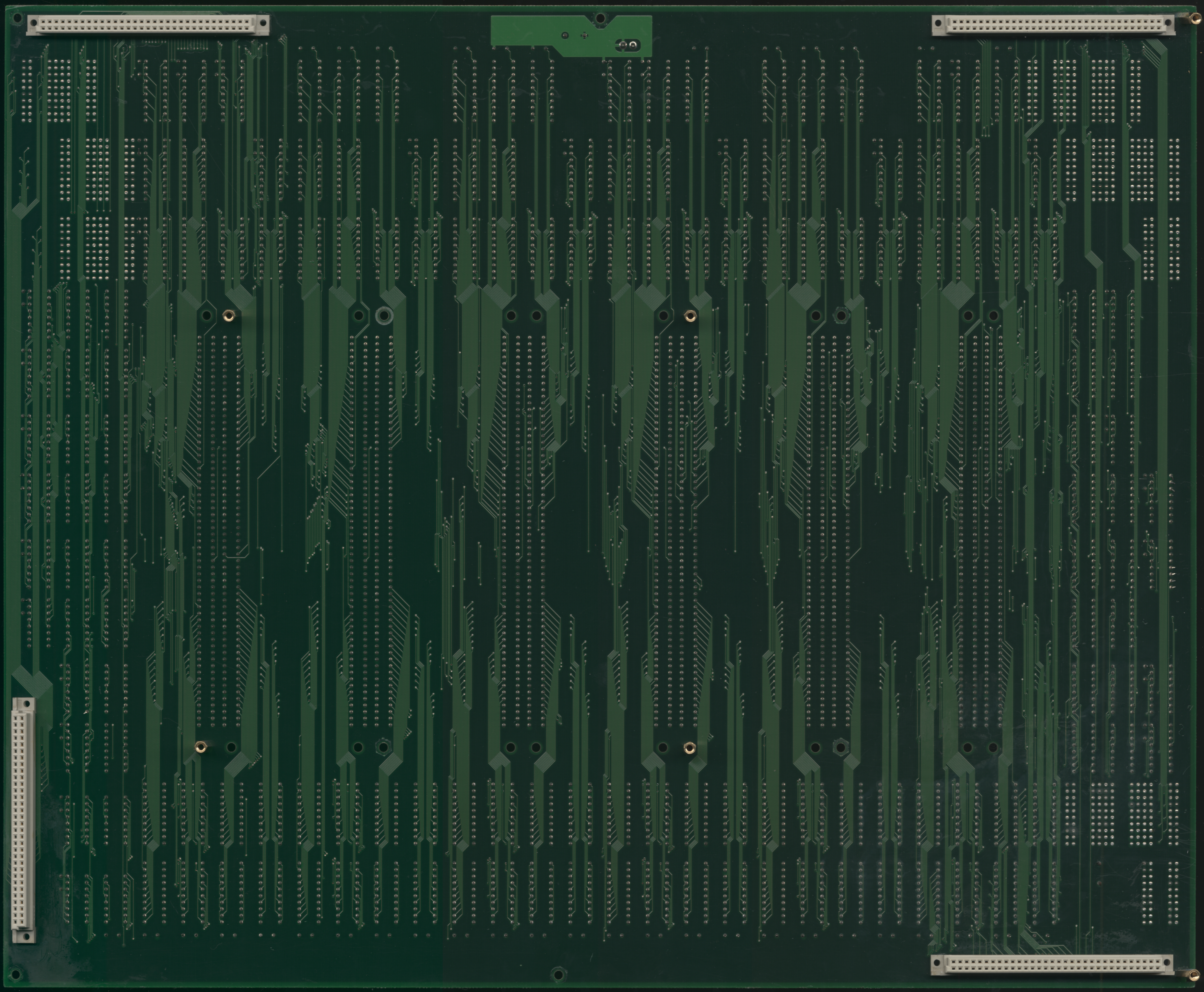
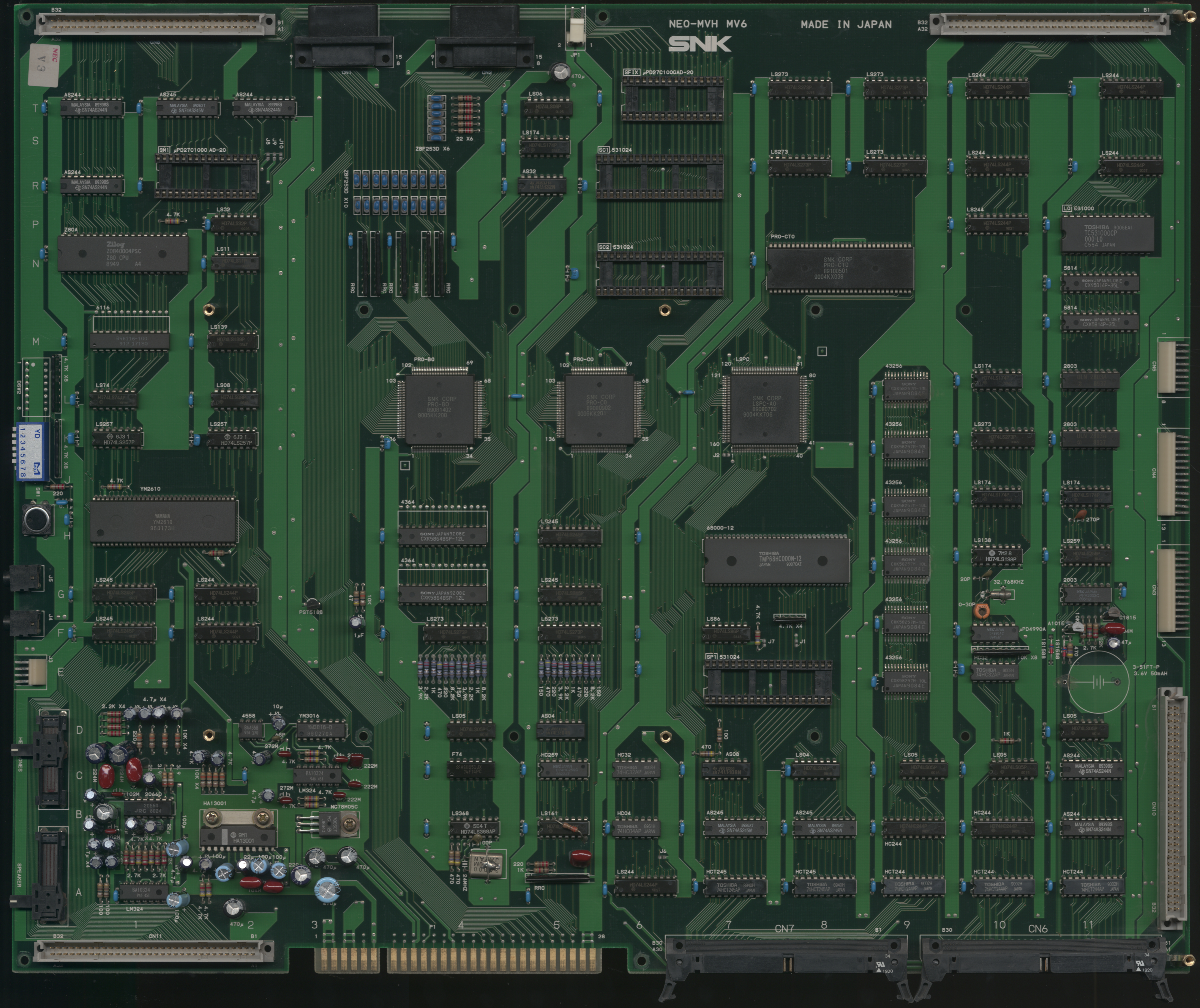
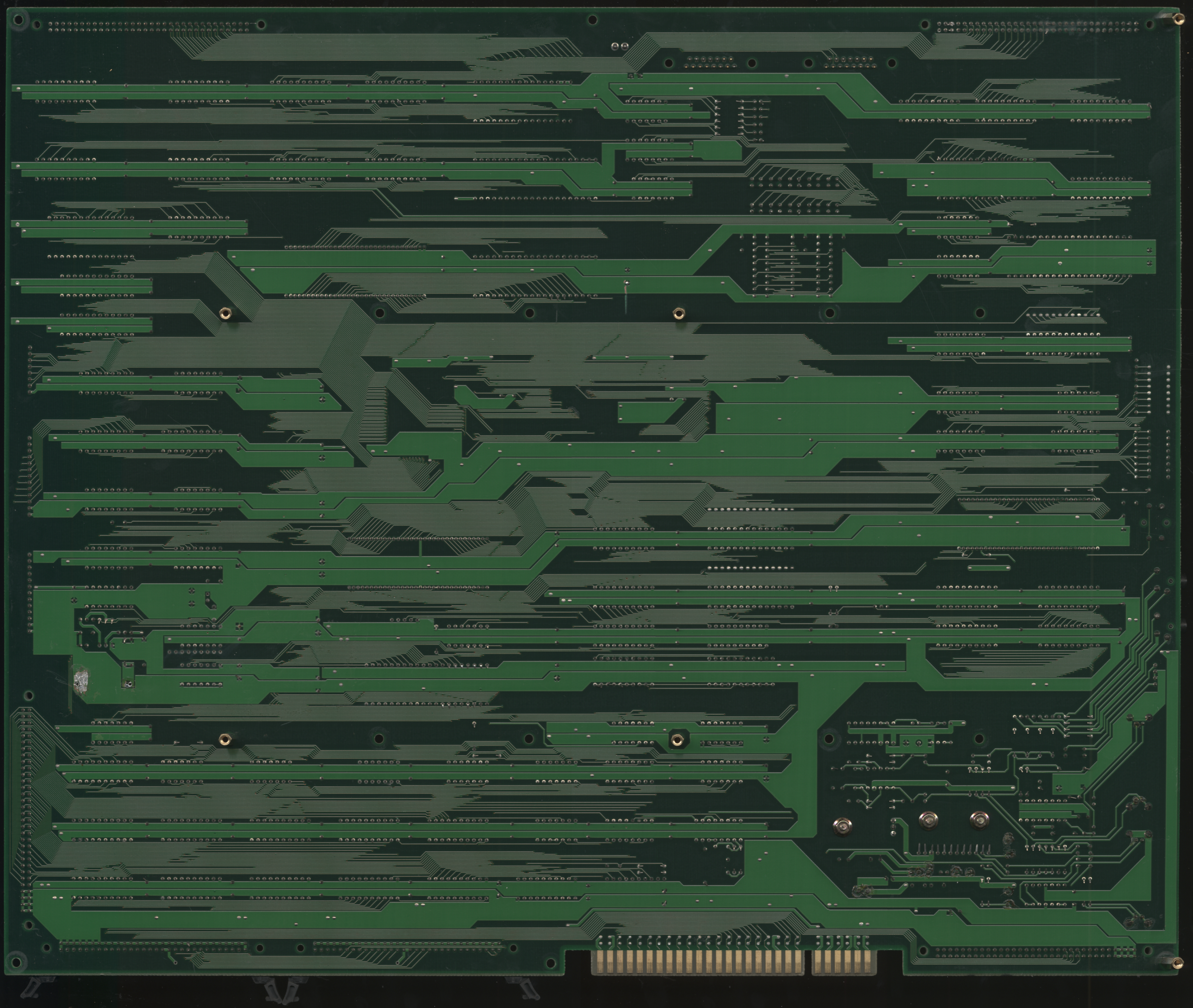
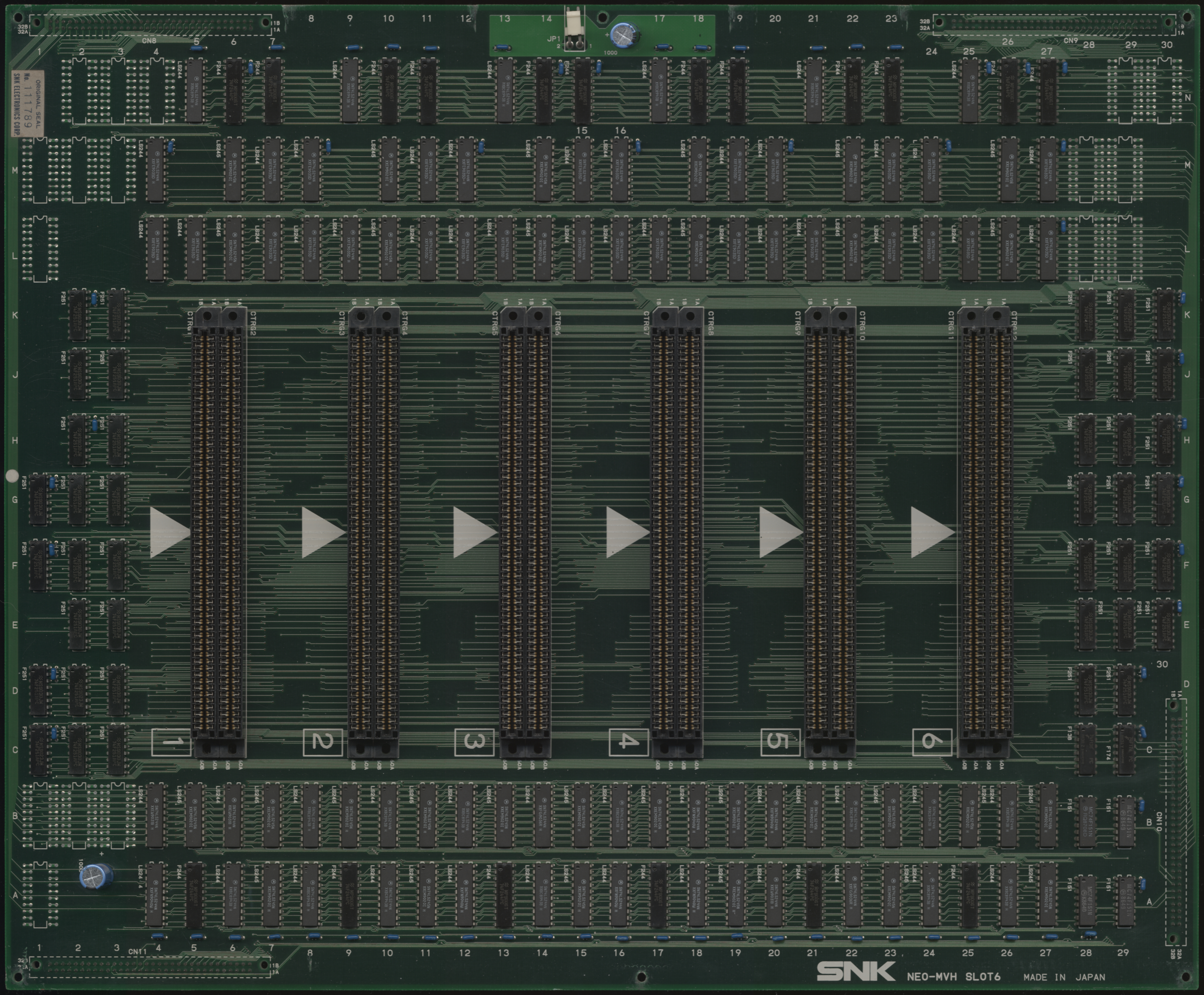
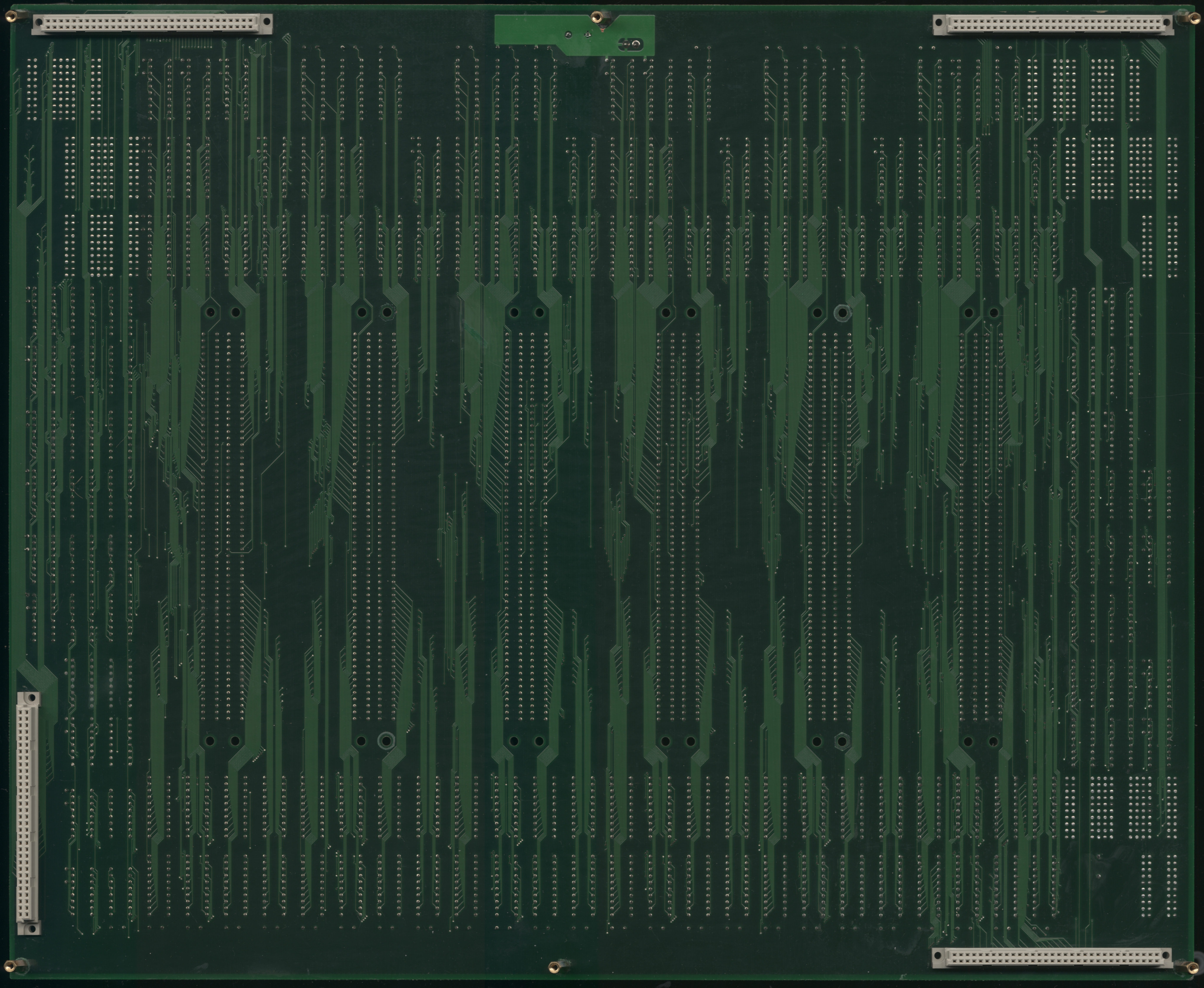
Board Scans - Set 1
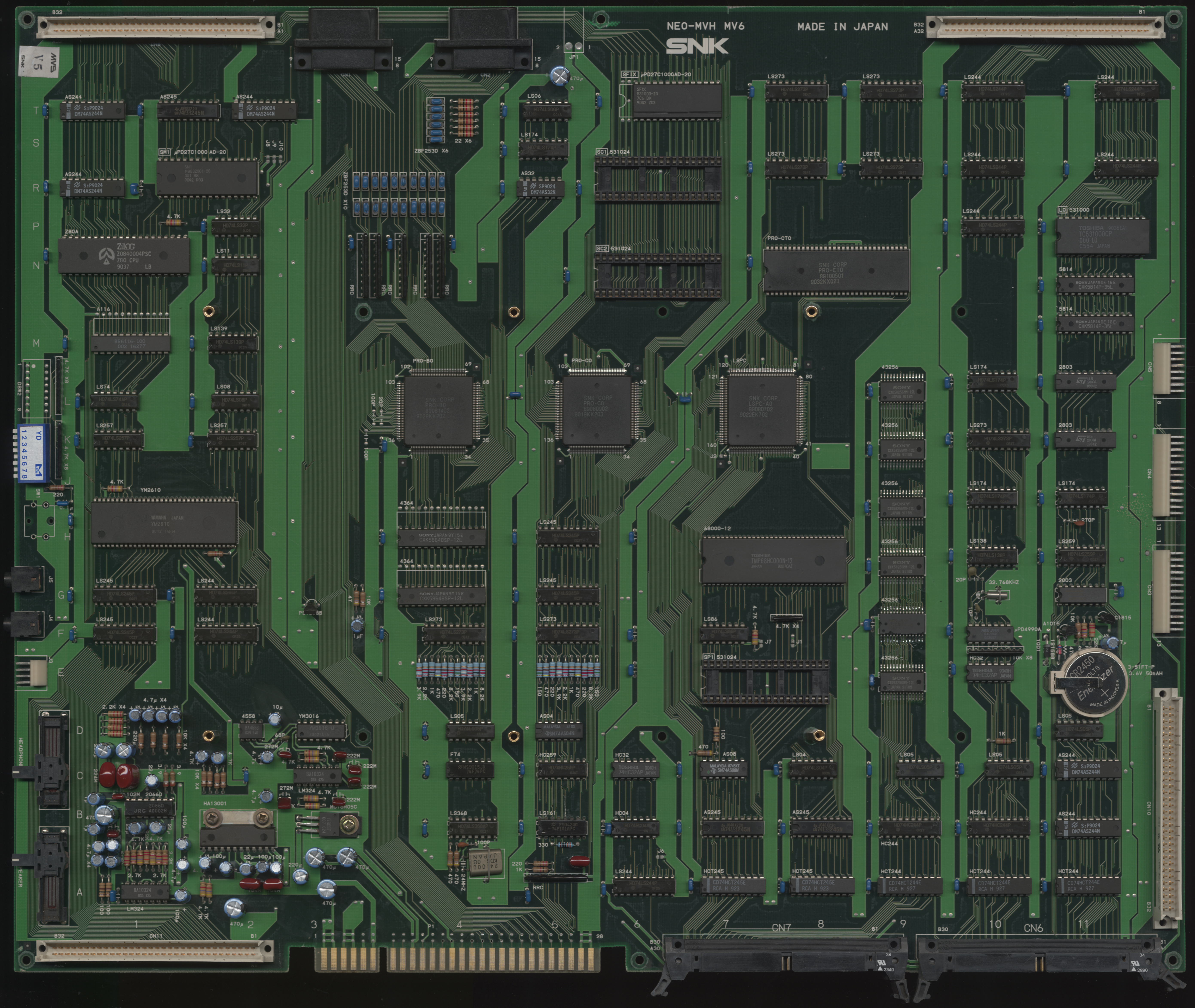
- The battery and BIOS chip were removed.
- The socketed SM1 and SFIX chips were removed (forgot to add them back before scanning).
- The sockets with label SC1 and SC2 below the SFIX were empty to begin with.
- Any metal stand offs seen the boards were use to level the board for scanning.
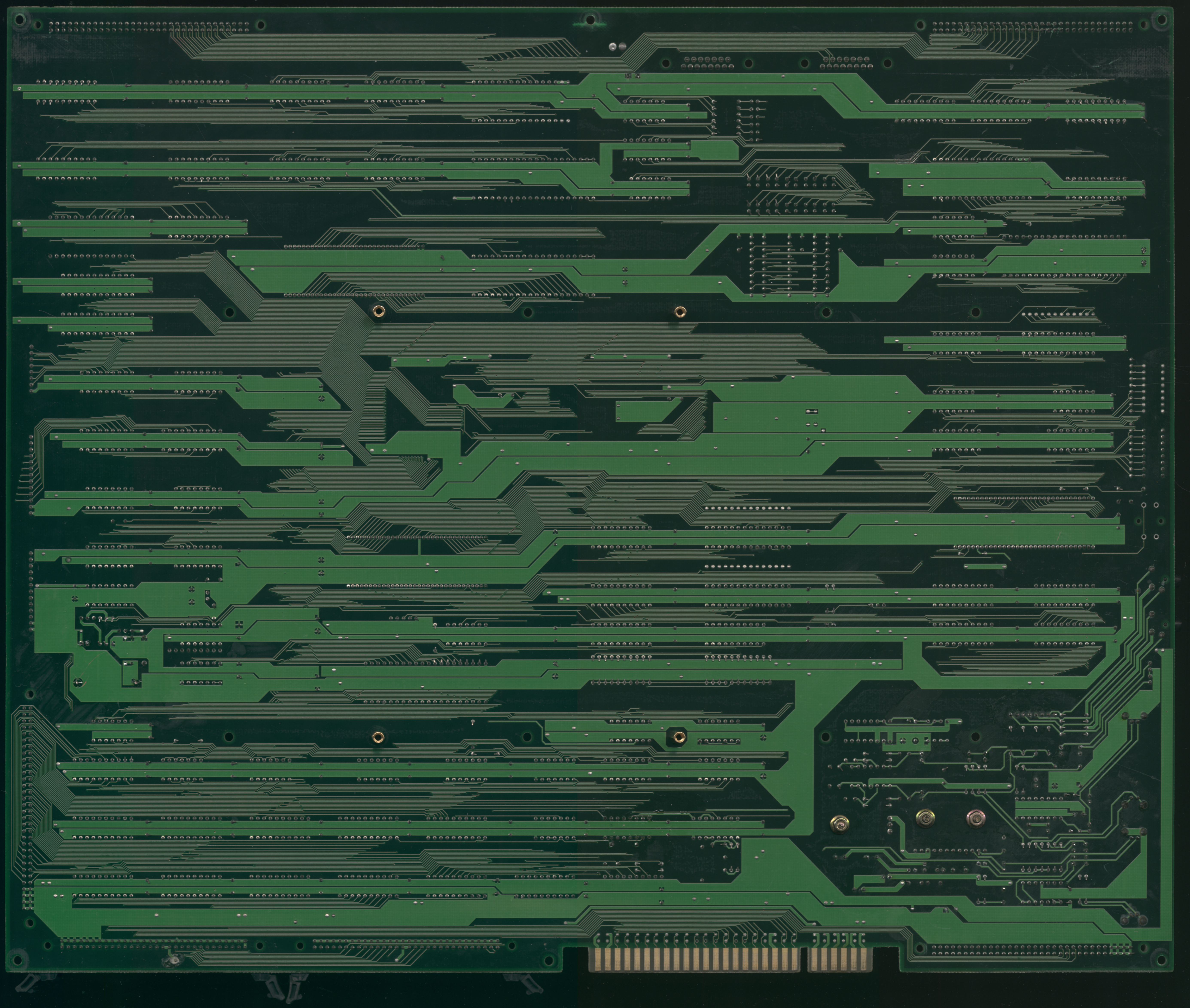
- Each image below is comprised of multiple scans stitched together.
Board Scans - Set 2
This is a newer revision of the MV6 board. The slot board looks the same but there are a number of minor updates/changes to the bottom/logic board.
- Reset switch (SW1) to the left of the YM2610 is gone
- Power connector (JP1) used to connect both boards is gone. The connector on the slot board is still here.
- The 330ohm hand added resistor on the LS161 @ B5 has been given a proper home below the chip
- The variable 0-30P capacitor (orange) above the uPD4990A @ G10 has been replaced by a normal 10P capacitor. Note that the old variable capacitor can cause a chirping sound.
- The distance between the positive and negative leads for the battery changed from 20mm (standard) to 23mm (non-standard)
- The left most 1S1588 diode next to the battery was replaced by at 10D1 diode. This is what other boards have.
- The 104M cap above the battery has been removed
